MTO stands for MOS turn-off thyristor. It is a high-power bipolar MOS thyristor that constitutes both MOSFET and Gate Turn-off thyristor (GTO). It was developed as a replacement for GTO. It is a latching device that outperforms MCT and IGBT when it comes to power and blocking voltages. It was developed by Silicon Power Company (SPCO) and operates similarly to the GTO except it can also go into an OFF state with a lower pulse current.
GTO can only go into an OFF state when a high pulse current is provided. In MTO the combination of MOSFET and GTO together allows it to switch off even with a low pulse current, therefore, overcoming the limitation of the GTO. A small signal voltage level needs to be provided to switch the MOSFET on.
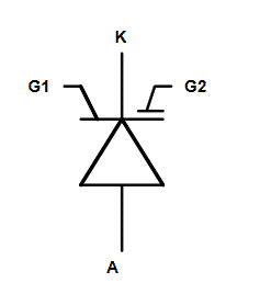
Figure 1 shows the symbol of MTO. It can be observed from the symbol that it has two gate terminals which are the turn-on gate (G1) and turn-off gate (G2) terminals. This is done to overcome the GTO limitation for the requirement of a high pulse current drive to switch off the thyristor.
Nowadays, they have high voltages up to 10 kV and high currents up to 4 kA. Due to this reason, they are being widely used in high power applications which range from 1-20 MVA.
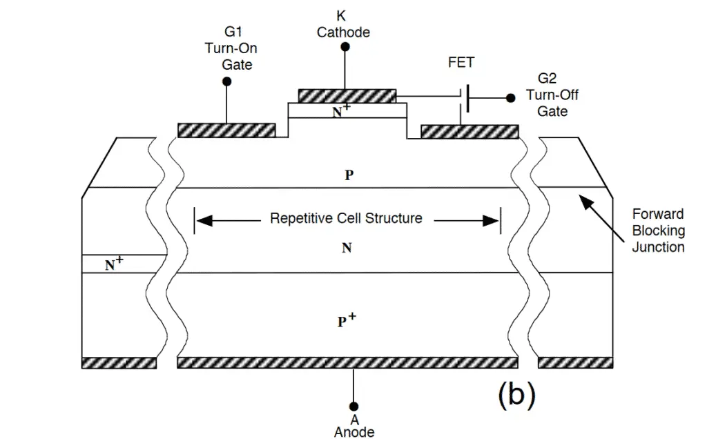
Structure of the MTO
The MTO is based on a four-layer latching structure. It has an ideal bi-stable switching behavior and has a low power dissipation in both On and Off states. To switch on the MTO a current pulse is applied at the turn-on gate (G1), which latches the device by switching the NPN transistor on. The collector current then provides base current to the lower PNP which results in switching the PNP transistor on which latches the MTO.
To turn off them, a gate voltage is applied at the MOSFET gate (Turn-off gate – G2). This turns on the MOSFET hence shorting the emitter and base of the MTO which stops the latching process. A gate turn-off thyristor (GTO) would have required a high current out of the emitter and base of the NPN transistor and a high negative pulse to stop the latching process. MTOs can turn off in 1-2 microseconds which makes them much faster and much efficient compared to GTOs.
MTO is much cheaper to construct and makes use of much smaller components for construction compared to the GTO, therefore, saving a lot of storage space.
Advantages
- It has a high power-rating ranging from 10 kV and 4 kA
- It requires smaller snubber components due to higher dv/dt.
- The cost of the components and gate driver power requirements is much lower than other turn-off devices.
Applications
The MTOs are usually used in high voltage applications of up to 20 MVA which require a fast gate turn-off switch. This is because it has a much ideal bi-stable switching behavior compared to other switching devices. Such applications include:
Uninterruptible power supplies for high power systems such as UPS
As the world progresses forward so does the requirement for uninterruptible power quality. UPSs are being used as a backup in applications such as computer service centers. Even though IGBT has been a viable switching device it has some drawbacks related to its packaging with respect to wire bond reliability and single-sided cooling. MTO is a better and reliable alternative than GTO and IGBT in high-power UPS applications.
Medium voltage motor drives
Ship propulsions, large fans, compressors, and pumps make use of variable speed drives for energy saving. The traditional custom design of medium voltage motor drives is expensive. With the high blocking voltage of the MTO, these drives can now be cheap and range from ratings between 2.3kV to 6.6kV. MTO also offers a much easier gate control mechanism making it a promising candidate for applications in these motor drives.
Reactive Harmonic compensators for utility
Many high-power converter applications such as flexible AC line transmission (FACT) have made use of GTO in multi-step configurations. MTO is now a much better candidate for carrying out the operation in the applications due to the low current gate driver, smaller snubber components and circuits, and the high switching speed due to low switching losses.
They are now in the market to make a phenomenal change in high-power DC/AC and DC/DC conversion and will eventually replace the GTO. They would allow a high power rating for switching devices.


very nicely explained
from where u get the references ?
can i get the link please