A Metal Oxide Semiconductor Field effect transistors, commonly known as MOSFET, are semiconductor switching devices that have three terminals which are the gate, drain and source. They are unipolar transistors, this means they depend on one type of charge carriers which can either be holes or electrons. They are much simpler to fabricate compared to bipolar junction transistors. They have a wide range of applications and are widely used in power electronic devices.
FET is made by growing a thin layer of Silicon dioxide over a semiconductor device which is nearly 0.1µm in thickness. When another metal oxide such as aluminium is deposited over the dielectric layer of silicon dioxide it makes the MOSFET. It has three terminals namely, gate, source and drain which have either the N-MOS channel or P-MOS channel.
Metal Oxide Semiconductor Field effect transistors gained their reliability in the 1980s and started challenging the reliability of bipolar transistors. Its low operating power requirements, switching speed, smaller size and high-frequency operations made them a better alternative to bipolar devices. Their switching speed capability exceeds several hundred kHz.
Physics behind the operation of MOSFET
Based on the construction, MOSFET can be classified into NMOS and PMOS. Lets us discuss the physics behind NMOS.
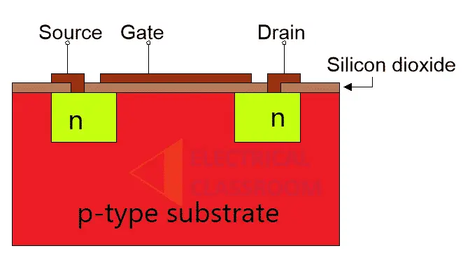
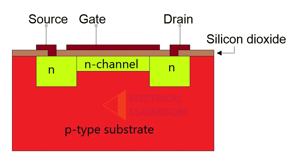
- NMOS consists of a lightly doped p-substrate, meaning that it has very less quantity of electrons, and two heavily doped n-type regions called as Source and drain. The source and drain terminals are interchangeable.
- The gate terminal is completely insulated from the p-type substrate by a silicon-oxide layer.
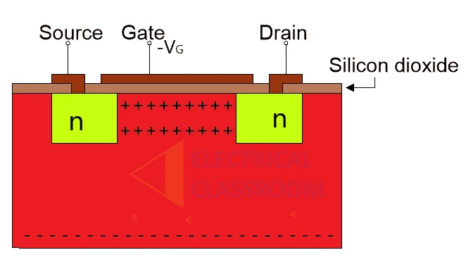
- When a negative voltage is applied to the gate terminal, an electric field is set up through the silicon-oxide layer.
- This electric field attracts the holes (positively charged majority carriers) towards the silicon-oxide layer and repels electrons (negatively charged minority carriers) away from it.
- At this point, the region below the the silicon-oxide layer lacks electrons.
- This region of charge accumulation is known as accumulation region
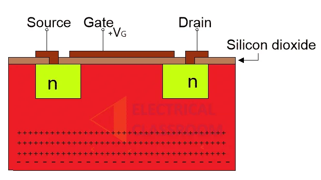
- At this point, if we apply a small positive gate voltage, holes are pushed away from the oxide. At the same time, the weak electric field will not be able to attract electrons toward the oxide region.
- Thus the region below the silicon dioxide layer lack any charged particles. This region of operation is called the depletion region.
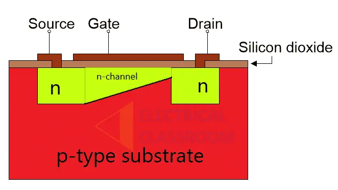
- At this point, if we increase the applied voltage, the electric field becomes strong enough to pull the electrons towards the silicon-oxide region. At a certain voltage, the concentration of electrons becomes so high that the region close to the silicon dioxide insulation becomes n-type.
- This region of operation is known as the inversion region.
- At this point, the inversion region connects the heavily doped source and drain regions and electrons can flow from the drain to the source through the inversion region.
Threshold voltage (Vt)
The gate voltage required to set up an inversion layer underneath the silicon-dioxide layer of the MOSFET is called as the threshold voltage. At this voltage, a channel of minority carriers is formed that connects the source to drain and enables current flow between the source and the drain.
Structure of MOSFET
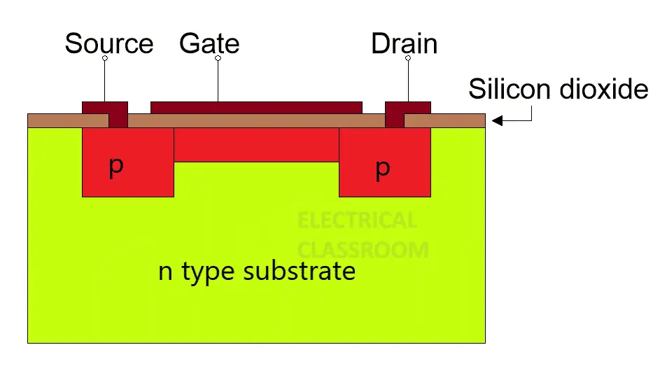
There are two construction types for each type which is the n-channel and p-channel. The material used to make the transistor is a polysilicon material which is a type of silicon metal that has a heavy concentration of charge carriers.
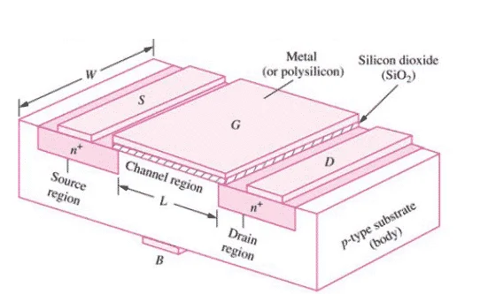
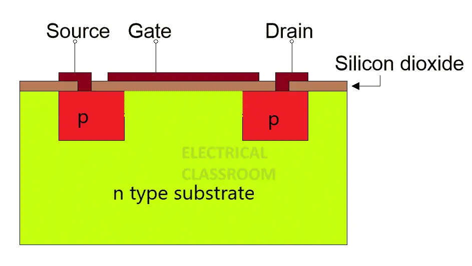
An MOSFET is a voltage controlled FET which has a metal oxide gate electrode. The gate is attached to the metal of the MOS structure. The gate electrode is separated from the main type of semiconductor which can either be the n-channel or p-channel by a thin insulating dielectric layer of silicon dioxide.
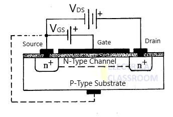
The p-type channel is doped with boron and the n-type channel is doped with phosphorus or arsenic. A pair of n-type regions can be seen just underneath the source and drain terminals.
The source and drain are one of the doped regions present on both sides of the MOS transistor where the source is the terminal with a lower potential and the drain is the terminal with a higher potential.
The body of the transistor is made of the substrate. In this figure, a p-type substrate is used. Three terminal voltages can be seen in the figure above which are:
- VGS: Gate to Source voltage
- VDS: Drain to Source voltage
- VBS: Body to Source voltage.
The gate is thick enough so that under AC or DC biasing conditions it can be an equipotential region. This means that it is possible to bias the gate of the MOSFET to either positive or negative polarity without any limitations. The insulated gate acts as one plate of a capacitor. This increases the overall input resistance of the MOSFET, therefore, making it almost infinite. This property of the MOSFET makes it a viable candidate for electronic switches or for making logic gates as with no bias and a high input resistance little or no input current is required.
There are no charge centres present in the oxide layer or oxide semiconductor interface. No current flows through the oxide layer under all the static biasing conditions as the oxide is a perfect insulator. This insulation prevents the current flow from the gate to the main current-carrying channel between the drain and source terminal. Therefore, no current flows into the gate.
The characteristics of the MOSFET resemble a voltage-controlled resistor. This is because the current flowing through the main channel between the source and drain is proportional to the input resistance. This makes the overall MOSFET input resistance very high which can cause large amounts of static charge to accumulate resulting in damaging the transistor.
The depletion and enhancement MOSFET make use of an electric field which is produced by the gate voltage to alter the flow of charge carriers. If it is an n-channel semiconductor device then electrons will flow and if it is a p-channel then holes will flow through the drain-source channel.
Operation of n-channel MOSFET
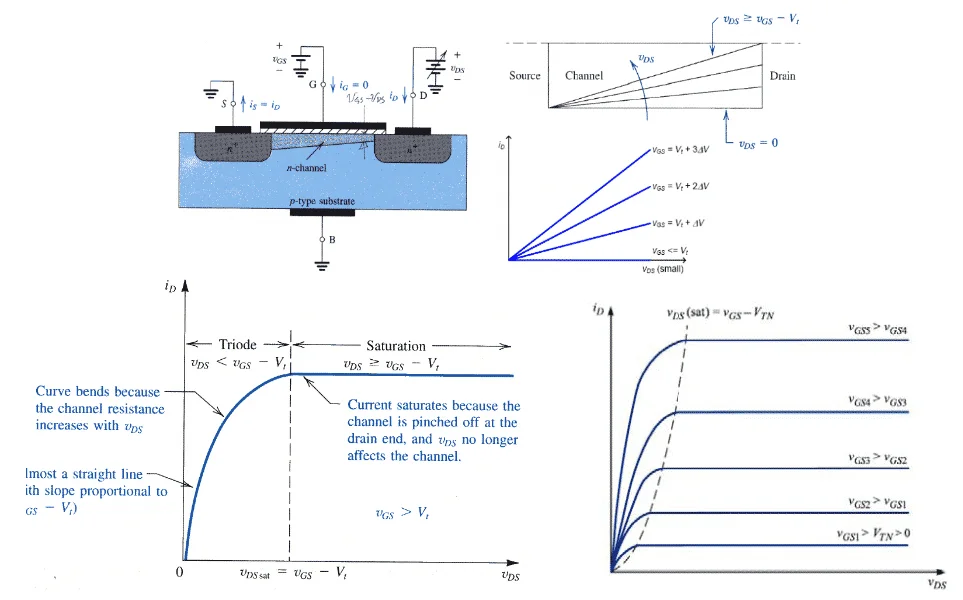
- When VDS = 0 and VGS = 0, MOSFET remains in the cutoff region and no current flows between source and drain.
- When VDS = 0 and 0 < VGS < Vt, the depletion region is formed.
- When VDS = 0 and VGS > Vt, the inversion region is formed and MOSFET will be ready to conduct.
- At this point of VDS is increased, current flows from drain to source and the IDS ∝ VDS.
- Increasing VGS further increases the electron density in the channel and also increases the conductivity between the source and drain.
MOSFET Symbol
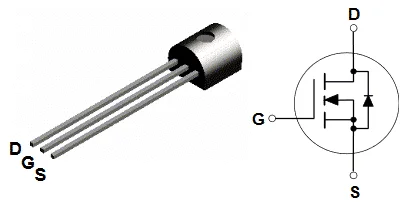
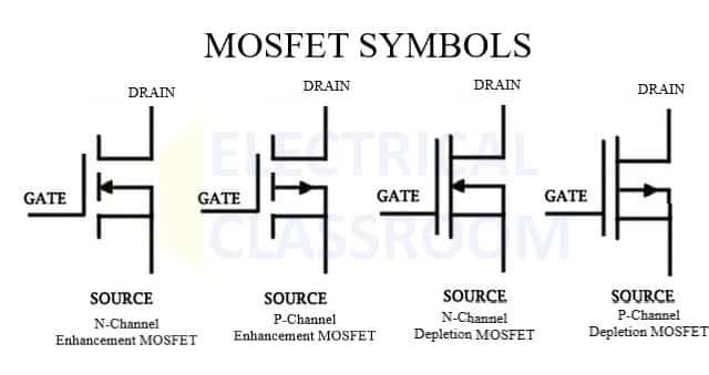
Figure 3 shows the four MOSFET symbols. The symbols show an additional terminal called the substrate. The substrate terminal is neither an input nor an output terminal but a terminal present to ground the substrate. It is used to connect the main semiconductive channel (n or p) through a diode junction to the metal layer of the MOSFET. It is at times connected internally to the source terminal. When such is the case it is removed from the symbol altogether.
The line between the drain (D) and source (S) connections show the semiconductive channel of the transistor. If the line is unbroken then it represents the Depletion type of MOSFET which is normally in an ON state as the drain current can flow with no gate biasing potential.
If the line is dotted or broken then it represents the Enhancement type of MOSFET which is normally in an OFF state as zero drain current flows with zero gate potential. Therefore, there is no voltage on the gate and the device does not conduct any current. The direction of the arrow represents whether the conductive channel is an N-type or P-type semiconductor device.
Based on the operation, two types of MOSFET:
- Depletion MOSFET
- Enhancement MOSFET
Depletion Mode MOSFET
This type of MOSFET is the least used transistor mode and is normally in an ON state when there is no gate bias voltage. This means that the channel would only conduct when VGS=0. The straight unbroken line in the symbol in figure 3 suggests that the depletion-mode MOSFET is considered a normally closed device that conducts when the conductive channel is closed.
In the n-channel depletion mode, when a negative gate-source voltage (-VGS) is applied, it depletes the conductive channel of its free electrons, therefore, switching the transistor “OFF”. Likewise in a p-channel depletion MOS transistor a positive gate-source voltage, +VGS depletes the conductive channels of its free holes, therefore, turning the transistor “OFF”.
Hence, if an n-channel depletion mode is used and the gate-source voltage is positive this would suggest that more electrons are allowed to roam freely, therefore, allowing more current to flow and vice versa would hold for p-channel depletion mode MOSFET. In a p-channel depletion mode MOSFET –VGS would mean fewer electrons are allowed to flow freely, therefore, increasing the total number of holes. This would mean less current would flow and this type of MOSFET would be considered a “normally-closed” switch.
Enhancement Mode MOSFET (eMOSFET)
The eMOSFET’s working principle is opposite to that of the depletion-mode MOSFET. In this type of transistor, the conducting channel is only lightly doped or sometimes not even doped which makes it non-conductive. Therefore, the device is normally in an OFF state which means it is non-conducting when the gate-bias voltage VGS=0. Its symbol consists of broken channel lines which illustrate that it is an open normally non-conducting channel.
When the n-channel is the conductive channel the eMOSFET will only allow the drain current to flow when a gate voltage (VGS) is applied at the gate terminals. The applied voltage needs to be greater than the threshold voltage V(TH) level in which the conductance takes place. This would make the semiconductor device a transconductance device.
When a positive voltage is applied to the gate in an n-channel device, more electrons are attracted towards the oxide layer present around the gate. This enhances the thickness of the channel which allows more current to flow. The increase in the positive voltage at the gate results in a decrease in channel resistance. This causes the drain current ID through the channel to increase. To summarise, for an n-channel eMOSFET, a positive VGS switches the transistor “ON” and a zero or –VGS switches the transistor “OFF”.
For a p-type eMOSFET, the device is in an “OFF” state when VGS=0 and the conductive channel is open. When a negative gate voltage (-VGS) is applied to the p-type eMOSFET, the channel conductivity increases therefore turning the transistor “ON”. This would mean for the transistor to be in an “OFF” state the applied voltage at the gate needs to be positive (+VGS).
Operating Region of P-channel eMOSFET
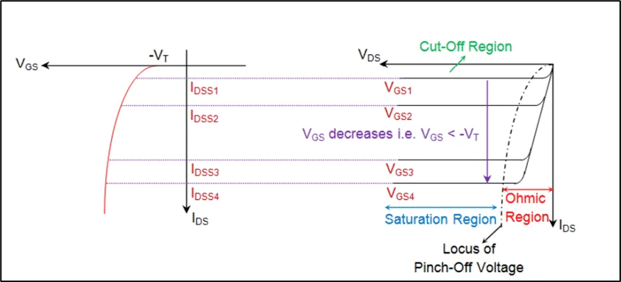
There are three operating regions for MOS transistors. They are the cut-off region, ohmic region and saturation region. IDS remains in its cut-off region that is zero when VGS becomes equal to –VT. This is important for establishing a connection between the drain terminal and the source terminal.
Once a connection is established the IDS increases in the reverse direction towards the source-drain terminal. This results in a reduction in the overall VDS value. Therefore, the device is now operating in the ohmic region where the current flowing through the device increases when an increased voltage(VDS) in the direction of source drain is applied.
When VDS becomes equal to –VP (pinch-off voltage or the gate-source voltage) the device enters into the saturation region. During this time a saturated amount of current (IDSS) flows through the device.
The amount of current that can flow is decided by the gate-source voltage (VGS). As the VGS becomes more negative, the saturation current increases. This can be observed in the figure above that the saturation current for VGS is much greater than VGS2. Also, as the negativity of the VGS increases the negativity of the pinch-off voltage (VP) increases proportionally.
Applications of MOSFET
Electronic Switches
eMOSFETs can be used as electronic switches as they have low “ON” resistance and their “OFF” resistance is very high. The input resistance is infinitely high due to the presence of an isolated gate which makes them an excellent candidate for electronic switches.
Logic Gates
eMOSFETs are also used in integrated circuits to produce power switching circuits as well as CMOS type logic gates. These are in the form of PMOS and NMOS gates. The logic device consists of both gates in the design.
Amplifier
Both depletion mode and enhancement mode MOSFET can be used to make single-stage class A amplifiers due to their high input resistance.
Review:
- Metal Oxide Semiconductor Field Effect Transistor is a voltage controlled unipolar switching device.
- It has a metal layer at the top, a silicon oxide insulation beneath that and a semiconductor part at the bottom giving it a vertical structure of p and n layers.
- Based on operation, MOSFETs are classified into Enhancement MOSFET (p-channel and n-channel) and depletion MOSFET (p-channel and n-channel).
- They have three terminals: Gate, Source and Drain.
- Gate acts as the control terminal and the actual conduction occurs between the source and the drains.
- Gate is insulated from the semiconductor layer by a thin layer of SiO2.
- Switching times of a MOSFET can be controlled completely by an external gate drive design.
Nice detailed explanations of the concepts!